BEAM-WAFER
The manufacturing and analysis of semiconductor products takes place on the sub-µm scale in many aspects. Ion implantation and layer deposition and growth typically reaches only a few 100 nm of depth/thickness. On these length scales, minute amount of dopants and impurities and exact knowledge of stoichiometries are of interest. Our BEAM-WAFER system enables quantification and depth-profiling of the implanted species with depth resolution down to the order of 10 nm. For c-RBS and lateral mappings the chamber can be equipped with a goniometer manipulator for handling all common wafer sizes (up to 450 mm) in translation and rotation. In addition to whole wafers these can also support numerous smaller pieces, e.g. for studying sample cut-outs after different diffusion steps. The analysis supports ion implantation, physical and chemical vapor deposition, atomic-layer deposition (ALD) and other processes.
IBA offers a unique properties for elemental tomography by providing extremely low detection limits. 1-4 MeV proton or heliums beams in combination with an optimised setup, including the right choice of detector apertures, detector sizes, and angles, enable RBS, NRA, PIXE, and PIGE to provide results for different elements and structures of interest to your applications. Consequently, IBA represents an in-house alternative to XRF by synchrotron light due to its intrinsically low background and good detection limits.
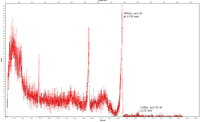
The spectrum on the right shows an example of trace element analysis in a boron doped industrial standard wafer with boron concentration in the ppm range. Also more complicated structures such as quantum dots or SiGe layers can be studied using IBA. IBA enables the analysis of deposited or grown layers down to monoatomic thicknesses and less with detection limits in the order of 1e17 atoms/m² or 0.1 ppm. In combination with other methods additional information can be derived such as density, porosity or surface coverage.
IBA also provides structural information via the so-called channeling-RBS (c-RBS). c-RBS enables the investigation of crystallinity via a reduction in stopping power for specific impact angles of the projectiles onto the crystalline channels. Crystalline defects represent obstacles to this channelling effect, enabling a quantification of the defect density in single crystals.